Thin film optical coatings are strongly present in semiconductors, AR (anti-reflection) or HR (highly reflective), optronic or photonic applications.
Generally, the composition of the films (major and impurities) as well as their structure and thickness must be precisely defined to obtain the good optical or other properties.
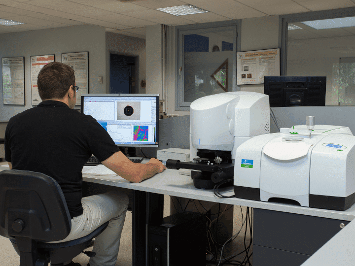
By combining the analytical means of Science and surface * and the laboratory of SERMA Technologies of Grenoble **, an exhaustive characterization of the surfaces and interfaces of multilayer materials composed of thin layers is possible.
* XPS, ToF-SIMS, GD-OES, MEB-FEG, FTIR microscopy, Profilometry,…
** FIB, MEB, TEM
Applications: optics, optronics, photonics, microelectronics, photovoltaics, mechanics…Thanks to a combination of powerful analytical tools, it is possible to determine and study:
- The number and nature of the layers,
- The thicknesses of the layers,
- Inter-layer migration or diffusion phenomena,
- Contamination on the surface and at interfaces.
The thickness of the thin layers can vary from the angstrom (Å / 10-10m), to the micron (µm / 10-6m), or even the millimeter (mm / 10-3m).
The sensitivity of the measurements varies according to the techniques, from atomic% to ppb (parts per billion / 10-9).
Thin layers can be analyzed in two different ways:
From the surface to the substrate:
The information obtained on the surface are roughness, morphology, surface composition and contaminants. By ionic abrasion, it is possible to access additional information, such as thickness, composition, depth distribution of elements and levels of dopants and contaminants.On a transverse section (MEB or ToF-SIMS) or on a thin transverse blade (TEM):
Sectional analyzes can reveal the thickness of the layers, the grain size, the composition and the crystallinity of the layers.Examples of basic depth distribution profile by ToF-SIMS and 3D imagery
- Tribological application:Structure of the multilayer, quality of the interfaces, spatial homogeneity
Example of TEM observation of an optical multilayer on a thin blade + structural analysis by electronic diffraction:
- Contamination and diffusion study:
Optical application: Demonstration of a diffusion at the interfaces and / or in the layers of trace elements (sodium (Na) and potassium (K)) and of the diffusion of oxide 2 in the oxide 1.
For any request for information:
Example of a basic depth distribution profile by GD-OES:
- Photovoltaic application:
► Determination of the number, nature of the layers and their thickness
► Diffusion of the element “X” at the interfaces
► Detection of trace elements (10 to 100 ppm)


